Nanofabrication of GaN vertical (V) nanowire (NW) MESFETs
| GaN V-NW MESFETs, i.e. Field-effect Transistors (FETs) with a Schottky barrier gate and channel consisting of GaN vertical nanowires (V-NWs), formed on a sapphire substrate, were realized and physically analyzed for the first time. This resulted in a validated nanofabrication technological platform for GaN V-NW devices that is comprehensively described in the published article, outcome of the PhD thesis research of Mr. George Doundoulakis, under the supervision of Prof. Alexandros Georgakilas and in collaboration with other members of the Microelectronics Research Group (MRG) of FORTH-IESL. The one-dimensional structure and the high aspect ratio of semiconductor nanowires render them highly desirable as building blocks for novel future devices in nanoelectronic, nanophotonic and sensor applications. Nanowire channel FETs with all-around gate, enable both ultimate channel nanoscaling and gate electrostatic control, as well as ultimate integration density, including 3D integration potential. This potential is well documented in the “International Roadmap for Devices and Systems (IRDS)” for the evolution of the Si CMOS digital logic technology, which also foresees the use of III-V semiconductor channel for N-type MOSFETs. To overcome complications of selective-area NW growth, the GaN NWs were formed by a top-down process, which combines conventional nanofabrication techniques and wet etching of a heteroepitaxial GaN epilayer grown on sapphire (0001) substrate. For practical reasons, the channel of the fabricated devices comprised an array of 900 GaN NWs with the narrowest reported diameter of 100 nm. The GaN V-NW MESFETs exhibited normally-off operation and threshold voltage of +0.4 V. Their operation was dominated by band bending and electron depletion toward the NW lateral sides, due to Schottky barrier at the gate and Fermi level pining by surface states at the source and drain access regions. A critical diameter (dcrit) for total NW depletion is defined by the lateral band bending and the NW carrier concentration. The presented V-NW FET nanofabrication process can be applicable for processing either single V-NW FETs as digital logic devices, or multiple V-NW FETs as high power GaN vertical transistor switches. From the same epitaxial structure with fixed concentration of donor impurities, different GaN NW diameters can provide both normally-on and normally-off transistors for logic circuits. Routes for further GaN V-NW FET device optimization were identified. Article: “Nanofabrication of normally-off GaN vertical nanowire MESFETs”, G. Doundoulakis, A. Adikimenakis, A. Stavrinidis, K. Tsagaraki, M. Androulidaki, F. Iacovella, G. Deligeorgis, G. Konstantinidis and A. Georgakilas, , Nanotechnology, vol. 30, no. 28, p. 285304, 2019 |
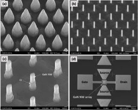
Figure: Scanning electron microscopy (SEM) images, in tilted-view, showing (a) the trapezoidal GaN NW array after reactive ion etching (RIE) of the GaN epilayer, (b) the final GaN NW array after RIE and anisotropic wet chemical etching, (c) the final GaN NW array after formation of Gate contact with length of 250 nm, and (d) the final fully-processed GaN V-NW MESFET |
January 2020